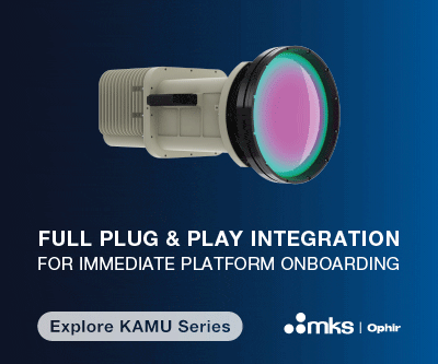

Optical Windows Lenses Domes
Discover cutting-edge solutions from leading global suppliersAyar Labs has been awarded a $15 million multi-year prototype Other Transaction Agreement (OTA) in support of Project KANAGAWA (the Co-Packaged Analog-Drive High-Bandwidth Optical Input/Output Project).
This project will promote the next-level development of Ayar Labs’ optical interconnects to lead its transition into the Defense Department’s advanced packaging ecosystem.
The OTA was issued by Naval Surface Warfare Center (NSWC), Crane Division to support the Office of the Under Secretary of Defense, Research & Engineering (OUSD(R&E)) Trusted & Assured Microelectronics (T&AM) program.
“We look forward to working closely with Ayar Labs as part of Project KANAGAWA to benchmark its optical I/O chiplets and lasers toward the transition of this technology into large-scale defense applications,” said Dr. Joshua Hawke, Chief Engineer of RF & Optoelectronics, NSWC Crane, Radar Technologies Division and Execution Lead of the OUSD(R&E) Trusted & Assured Microelectronics program.
During the first phase of Project KANAGAWA (Task A), Ayar Labs will deliver its optical I/O chiplets and lasers at data rate bandwidth levels exceeding 2 Tbps and energy losses below 5pJ/bit.
In phase two of the project, running parallel to Task A, Ayar Labs will collaborate with Intel, Lockheed Martin and Qorvo to develop and demonstrate co-packaged optical I/O solutions built on TeraPHY optical I/O chiplets and SuperNova multi-wavelength lasers, with the goal of advancing the supply chain ecosystem for domestic manufacturing of Ayar Labs’ optical I/O solution.
“Project KANAGAWA comes at an important time for both our nation and Ayar Labs as we look to mature US-based manufacturing for our optical I/O solutions,” said Charles Wuischpard, CEO of Ayar Labs. “We are excited to partner with the DoD, Intel, Lockheed Martin and Qorvo to not only strengthen our nation’s security by establishing domestic production of our optical I/O chiplets but also introduce next-generation defense architectures and systems.”
Co-packaged optics, which bring together photonic integrated circuits with electronic integrated circuits inside multi-chip packages, extend the reach of high-bandwidth data I/O. Ayar Labs believes MCPs leveraging the comany’s optical I/O are poised to significantly expand the capabilities of defense microelectronics. For example, this technology can generate dramatically higher data rates from the field-programmable gate arrays that process digital beamforming signals, opening the door to new phased array radar architectures.